Illuminating Profits: A Comprehensive Cost Model for LED Chip Manufacturing

The LED chip is the core component of an LED bulb, comprising semiconductor layers that enable the free flow of protons and electrons. Found in all LED lighting fixtures—from bulbs to tubes—the LED chip fundamentally determines light quality, with variations in brightness, voltage, and wavelength. These chips are manufactured through a process called MOCVD (metal-organic chemical vapor deposition), which creates the semiconductor layers that facilitate electric flow. When an LED chip is connected to a power source, voltage is applied in both forward and reverse directions, causing electrons and holes to move within the chip and generate a current. As electrons and holes of opposite charges meet, they combine in a process called recombination. During recombination, the energy produced is less than that of the individual electrons and holes, with the excess energy converted into light, resulting in light emission. Major applications of these chips include backlighting, illumination, automotive lighting, signs, and signals.
The global LED chip market was valued at USD 31.26 Billion in 2024. According to IMARC Group, the market is projected to reach USD 81.67 Billion by 2033, growing at a CAGR of 10.70% from 2025 to 2033. The market is primarily driven by a growing preference for cost-effective lighting solutions and increasing awareness of energy conservation, which significantly boosts demand for these products. LED chips efficiently convert electricity into energy with minimal waste while providing high luminous intensity. Furthermore, ongoing technological advancements and extensive research and development (R&D) efforts have reduced the average cost of LEDs, which serves as a key growth driver. Additionally, various governments worldwide are promoting energy-efficient lighting solutions, further supporting LED chip sales. Rapid urbanization, robust growth in the real estate sector, and rising disposable incomes are also contributing to a positive global market outlook.
It is also driven by the development of effective and reliable low-ohmic contact electrodes. These electrodes help maintain a minimal voltage drop between contact materials and provide stable bonding pads for wires while maximizing light emission. Additionally, innovation has propelled market demand, with companies introducing advanced products to meet evolving needs. For example, in 2020, Osram launched its projector power series of LED chips, delivering brightness of 1000 ANSI lumens. Such advancements have broadened applications across various industries, supporting global market growth.
Trending Insights on LED Chip: Latest News and Developments
- In January 2025, San'an Optoelectronics, a Chinese manufacturer, is increasing its production capacity in response to the growing demand for its microLED wafers. By the end of the quarter, San'an will have increased its monthly production capacity to 1,400 6" microLED wafers from its present capacity of 250.
- In December 2024, Tianma declared that their Micro LED production line had successfully integrated its whole process. Tianma plans to increase production in 2025 after completing full-process integration for its micro-LED plant. It focusses on applications for automobile displays.
- In December 2024, VISTAR unveiled its first mass-produced product and announced the opening of the first TFT-based Micro LED mass production line on the Chinese mainland. This milestone gives the nascent display sector tremendous impetus and signifies a breakthrough in Micro LED display technology.
- In August 2023,China-based BOE HC Semitek began construction of a US$ 700 million microLED epiwafer production line in Zhuhai, China's Jinwan District. The business declared that it has begun manufacturing sample wafers in October 2024.
Case Study on Cost Model of LED Chip Manufacturing Plant
One of our clients reached out to us to conduct a feasibility study for setting up a large-scale LED chips manufacturing plant. We developed a comprehensive financial model for the setup and operation of a proposed LED chip manufacturing plant in India. This plant is designed to produce approximately 336 wafers, or around 12,000 LED chips per day.
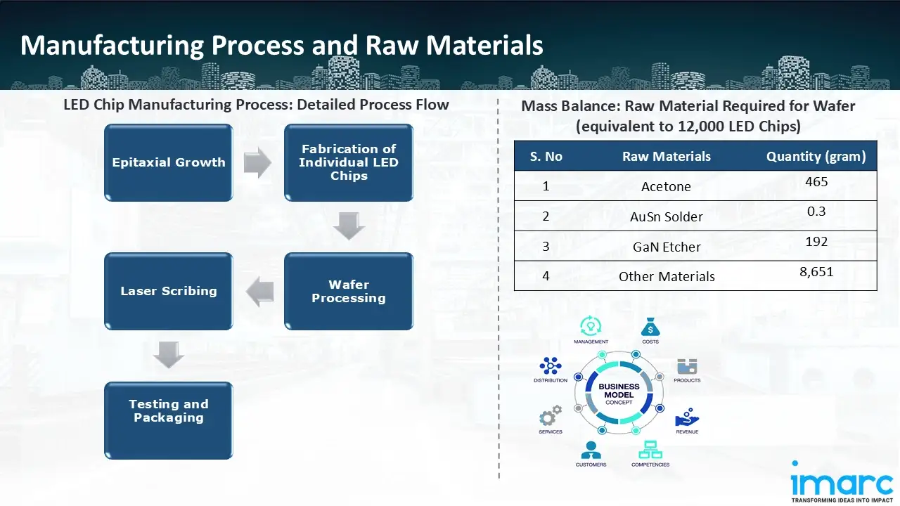
Manufacturing Process: LED chip manufacturing spans several stages: epitaxial growth, chip fabrication, wafer processing, and backend processing. Epitaxial growth uses MOCVD technology to form layers in the LED structure, such as the GaN buffer and MQW active region, enhancing LED performance through improved process control, gas flow, and temperature uniformity. In the chip fabrication stage, semiconductor layers are patterned, and metal layers are deposited to create electrical contacts, followed by surface texturing to improve light extraction. Wafer processing includes p-contact layer formation, mesa etching for n-GaN exposure, and metallization, providing connections to the LED package. The wafer is then thinned, usually by grinding and laser lift-off. Backend processing involves die singulation and testing. During laser scribing, the wafer is prepared for individual die separation with precision. Next, film frame mounters hold the wafer during singulation, while die expanders stretch it for testing and placement. This process enables efficient LED chip production, ensuring consistent quality and performance.

Mass Balance and Raw Material Required: The primary raw materials used in the LED chips manufacturing plant include acetone, AuSn solder, GaN etchant, developer, etcher Ag, etchant metal, zeolite slurry, hydrogen gas, nitrogen gas, ammonia, oxygen gas, and various other components. For a plant producing wafer (equivalent to 12,000 LED chips), the required quantities are as follows: acetone (467 g), AuSn solder (0.3 g), GaN etchant (192 g), and other materials (8,651 g).
List of Machinery:
The following equipment was required for the proposed plant:
- MOCVD
- Lithography Machine
- Plasma Etcher
- Laser Lift off
- Laser Scriber
- Breaker
- Film Mounter
- Die Expander
- UV Tape UV Curing Systems
- Ultrapure Water Purification System
Techno-Commercial Parameter:
- Capital Investment (CapEx): Capital expenditure (CapEx) in a manufacturing plant includes various investments essential for its setup and long-term operations. It covers machinery and equipment costs, including procurement, installation, and commissioning. Civil works expenses involve land development, factory construction, and infrastructure setup. Utilities such as power, water supply, and HVAC systems are also significant. Additionally, material handling systems, automation, environmental compliance, and safety measures are key components. Other expenditures include IT infrastructure, security systems, and office essentials, ensuring operational efficiency and business growth.
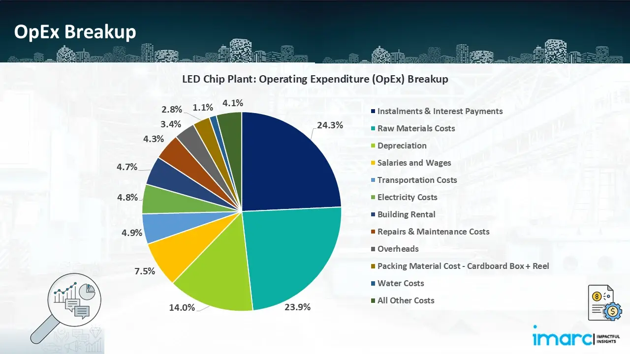
- Operating Expenditure (OpEx): Operating expenditure is the cost incurred to operate a manufacturing plant effectively. Opex in a manufacturing plant typically includes the cost of raw materials, utilities, depreciation, taxes, packing cost, transportation cost, and repairs and maintenance. The operating expenses are part of the cost structure of a manufacturing plant and have a significant effect on profitability and efficiency. Effective control of these costs is necessary for maintaining competitiveness and growth.

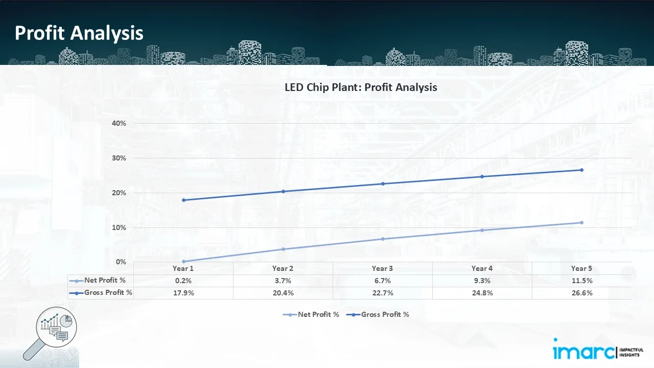
- Profitability Analysis Year on Year Basis: The proposed LED chip plant, with a capacity of approximately 336 wafers, or around 12,000 LED chips per day, achieved an impressive revenue of INR 245.7 million in its first year. We assisted our client in developing a detailed cost model, which projects steady growth, with revenue rising throughout the projected period. Moreover, gross profit margins improve from 17.9% to 26.6% by year 5, and net profit rises from 0.2% to 11.5%, highlighting strong financial viability and profitability.

Conclusion
Our financial model for the LED chips manufacturing plant was meticulously developed to meet the client’s objectives, providing an in-depth analysis of production costs, including raw materials, manufacturing, capital expenditure, and operational expenses. By addressing the specific requirements of producing 336 wafers per day, we successfully identified key cost drivers and projected profitability, considering market trends, inflation, and potential fluctuations in raw material prices. This comprehensive financial model equipped the client with valuable insights for strategic decision-making, demonstrating our commitment to delivering high-quality, client-focused solutions that ensure the long-term success of large-scale manufacturing ventures.
IMARC's Financial Model Expertise: Helping Our Clients Explore Industry Economics
IMARC is a global market research company that offers a wide range of services, including market entry and expansion, market entry and opportunity assessment, competitive intelligence and benchmarking, procurement research, pricing and cost research, regulatory approvals and licensing, factory setup, factory auditing, company incorporation, incubation services, recruitment services, and marketing and sales.
Under our factory setup services, we assist our clients in exploring the feasibility of their plants by providing comprehensive financial modeling. Additionally, we offer end-to-end consultation for setting up a plant in India or abroad. Our financial modeling includes an analysis of capital expenditure (CapEx) required to establish the manufacturing facility, covering costs such as land acquisition, building infrastructure, purchasing high-tech production equipment, and installation. Furthermore, the layout and design of the factory significantly influence operational efficiency, energy consumption, and labor productivity, all of which impact long-term operational expenditure (OpEx). So, every parameter is covered in the analysis.
At IMARC, we leverage our comprehensive market research expertise to support companies in every aspect of their business journey, from market entry and expansion to operational efficiency and innovation. By integrating our factory setup services with our deep knowledge of industry dynamics, we empower our clients to not only establish manufacturing facilities but also strategically position themselves in highly competitive markets. Our financial modeling and end-to-end consultation services ensure that clients can explore the feasibility of their plant setups while also gaining insights into competitors' strategies, technological advancements, and regulatory landscapes. This holistic approach enables our clients to make informed decisions, optimize their operations, and align with sustainable practices, ultimately driving long-term success and growth.
Our Clients
Contact Us
Have a question or need assistance?
Please complete the form with your inquiry or reach out to us at
Phone Number
+91-120-433-0800+1-201-971-6302
+44-753-714-6104


